- 您现在的位置:买卖IC网 > Sheet目录3832 > PIC16F876A-I/ML (Microchip Technology)IC MCU FLASH 8KX14 A/D 28QFN
2003 Microchip Technology Inc.
DS39582B-page 133
PIC16F87XA
11.5
A/D Operation During Sleep
The A/D module can operate during Sleep mode. This
requires that the A/D clock source be set to RC
(ADCS1:ADCS0 = 11). When the RC clock source is
selected, the A/D module waits one instruction cycle
before starting the conversion. This allows the SLEEP
instruction to be executed which eliminates all digital
switching noise from the conversion. When the conver-
sion is completed, the GO/DONE bit will be cleared and
the result loaded into the ADRES register. If the A/D
interrupt is enabled, the device will wake-up from
Sleep. If the A/D interrupt is not enabled, the A/D mod-
ule will then be turned off, although the ADON bit will
remain set.
When the A/D clock source is another clock option (not
RC), a SLEEP instruction will cause the present conver-
sion to be aborted and the A/D module to be turned off,
though the ADON bit will remain set.
Turning off the A/D places the A/D module in its lowest
current consumption state.
11.6
Effects of a Reset
A device Reset forces all registers to their Reset state.
This forces the A/D module to be turned off and any
conversion is aborted. All A/D input pins are configured
as analog inputs.
The value that is in the ADRESH:ADRESL registers is
not
modified
for
a
Power-on
Reset.
The
ADRESH:ADRESL registers will contain unknown data
after a Power-on Reset.
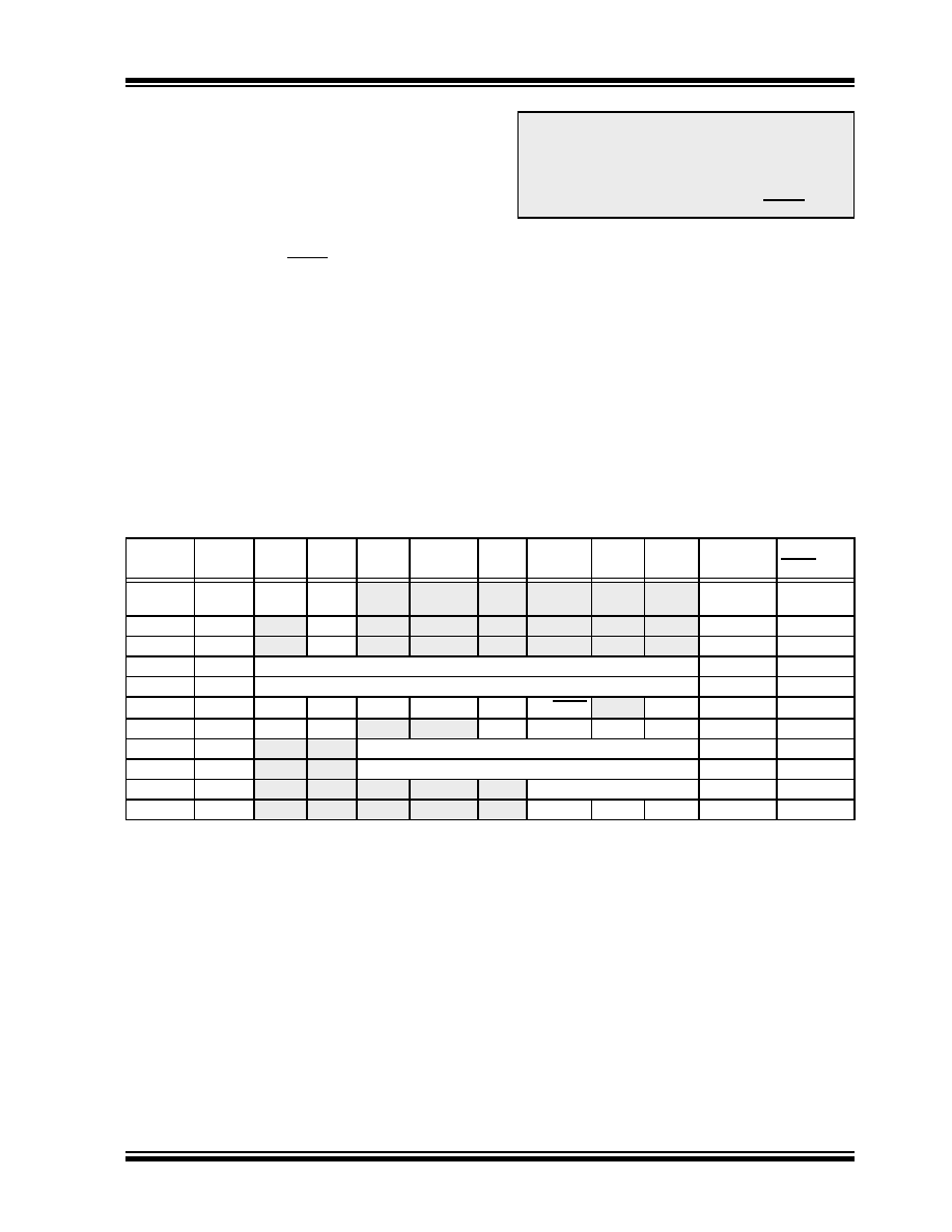
TABLE 11-2:
REGISTERS/BITS ASSOCIATED WITH A/D
Note:
For the A/D module to operate in Sleep,
the A/D clock source must be set to RC
(ADCS1:ADCS0 = 11). To allow the con-
version to occur during Sleep, ensure the
SLEEP
instruction immediately follows the
instruction that sets the GO/DONE bit.
Address
Name
Bit 7
Bit 6
Bit 5
Bit 4
Bit 3
Bit 2
Bit 1
Bit 0
Value on
POR, BOR
Value on
MCLR, WDT
0Bh,8Bh,
10Bh,18Bh
INTCON
GIE
PEIE
TMR0IE
INTE
RBIE
TMR0IF
INTF
RBIF
0000 000x
0000 000u
0Ch
PIR1
PSPIF(1)
ADIF
RCIF
TXIF
SSPIF
CCP1IF
TMR2IF TMR1IF 0000 0000 0000 0000
8Ch
PIE1
PSPIE(1)
ADIE
RCIE
TXIE
SSPIE
CCP1IE
TMR2IE TMR1IE 0000 0000 0000 0000
1Eh
ADRESH A/D Result Register High Byte
xxxx xxxx
uuuu uuuu
9Eh
ADRESL
A/D Result Register Low Byte
xxxx xxxx
uuuu uuuu
1Fh
ADCON0
ADCS1
ADCS0
CHS2
CHS1
CHS0
GO/DONE
—ADON
0000 00-0
9Fh
ADCON1
ADFM
ADCS2
—
PCFG3
PCFG2
PCFG1
PCFG0
00-- 0000
85h
TRISA
—
PORTA Data Direction Register
--11 1111
05h
PORTA
—
PORTA Data Latch when written: PORTA pins when read
--0x 0000
--0u 0000
89h(1)
TRISE
IBF
OBF
IBOV
PSPMODE
—
PORTE Data Direction bits
0000 -111
09h(1)
PORTE
—
RE2
RE1
RE0
---- -xxx
---- -uuu
Legend:
x
= unknown, u = unchanged, - = unimplemented, read as ‘0’. Shaded cells are not used for A/D conversion.
Note
1:
These registers are not available on 28-pin devices.
发布紧急采购,3分钟左右您将得到回复。
相关PDF资料
PIC16F876A-I/SO
IC MCU FLASH 8KX14 EE 28SOIC
PIC16F876A-I/SP
IC MCU FLASH 8KX14 EE 28DIP
AT87C51RD2-3CSUM
IC 8051 MCU 64K OTP 40MHZ 40DIP
DSPIC33FJ64MC802-I/SO
IC DSPIC MCU/DSP 64K 28-SOIC
DSPIC33FJ64GP802-I/MM
IC DSPIC MCU/DSP 64K 28-QFN
AT87C51RD2-3CSUL
IC 8051 MCU 64K OTP 30MHZ 40DIP
PIC18F2431-I/SP
IC PIC MCU FLASH 8KX16 28DIP
AT87C51RC2-SLSUM
IC 8051 MCU 32K OTP 40MHZ 44PLCC
相关代理商/技术参数
PIC16F876A-I/ML
制造商:Microchip Technology Inc 功能描述:IC 8BIT FLASH MCU SMD 制造商:Microchip Technology Inc 功能描述:IC, 8BIT FLASH MCU, SMD
PIC16F876A-I/MLG
功能描述:8位微控制器 -MCU 14KB 368 RAM 22 I/O Lead Free Package RoHS:否 制造商:Silicon Labs 核心:8051 处理器系列:C8051F39x 数据总线宽度:8 bit 最大时钟频率:50 MHz 程序存储器大小:16 KB 数据 RAM 大小:1 KB 片上 ADC:Yes 工作电源电压:1.8 V to 3.6 V 工作温度范围:- 40 C to + 105 C 封装 / 箱体:QFN-20 安装风格:SMD/SMT
PIC16F876A-I/SO
功能描述:8位微控制器 -MCU 14KB 368 RAM 22 I/O RoHS:否 制造商:Silicon Labs 核心:8051 处理器系列:C8051F39x 数据总线宽度:8 bit 最大时钟频率:50 MHz 程序存储器大小:16 KB 数据 RAM 大小:1 KB 片上 ADC:Yes 工作电源电压:1.8 V to 3.6 V 工作温度范围:- 40 C to + 105 C 封装 / 箱体:QFN-20 安装风格:SMD/SMT
PIC16F876A-I/SO
制造商:Microchip Technology Inc 功能描述:8BIT FLASH MCU SMD 16F876 SOIC28
PIC16F876A-I/SOE3
制造商:Microchip Technology Inc 功能描述:8-BIT, FLASH, 20 MHz, RISC MICROCONTROLLER, 28 Pin Plastic SMT
PIC16F876A-I/SOG
功能描述:8位微控制器 -MCU 14KB 368 RAM 22 I/O RoHS:否 制造商:Silicon Labs 核心:8051 处理器系列:C8051F39x 数据总线宽度:8 bit 最大时钟频率:50 MHz 程序存储器大小:16 KB 数据 RAM 大小:1 KB 片上 ADC:Yes 工作电源电压:1.8 V to 3.6 V 工作温度范围:- 40 C to + 105 C 封装 / 箱体:QFN-20 安装风格:SMD/SMT
PIC16F876A-I/SP
功能描述:8位微控制器 -MCU 14KB 368 RAM 22 I/O RoHS:否 制造商:Silicon Labs 核心:8051 处理器系列:C8051F39x 数据总线宽度:8 bit 最大时钟频率:50 MHz 程序存储器大小:16 KB 数据 RAM 大小:1 KB 片上 ADC:Yes 工作电源电压:1.8 V to 3.6 V 工作温度范围:- 40 C to + 105 C 封装 / 箱体:QFN-20 安装风格:SMD/SMT
PIC16F876A-I/SP
制造商:Microchip Technology Inc 功能描述:IC 8BIT FLASH MCU 16F876 SDIL28